- The realisation that a global silicon order is incomplete without India’s scale and talent has led to a formal invitation for India to join the Pax Silica pact.
- The iCET 2.0 framework is focused on eliminating the ‘regulatory cholesterol’ that has historically affected hi-tech commerce between Washington and New Delhi.
- India benefits from participating in the Pax Silica framework via iCET 2.0 in that it enjoys “strategic insurance”.
- India has shifted from a passive observer to a key player in the global semiconductor race, using iCET 2.0 to drive international partnerships and ISM 2.0 to strengthen domestic capacity, cementing its role as the Indo-Pacific’s “Silicon Sentinel.
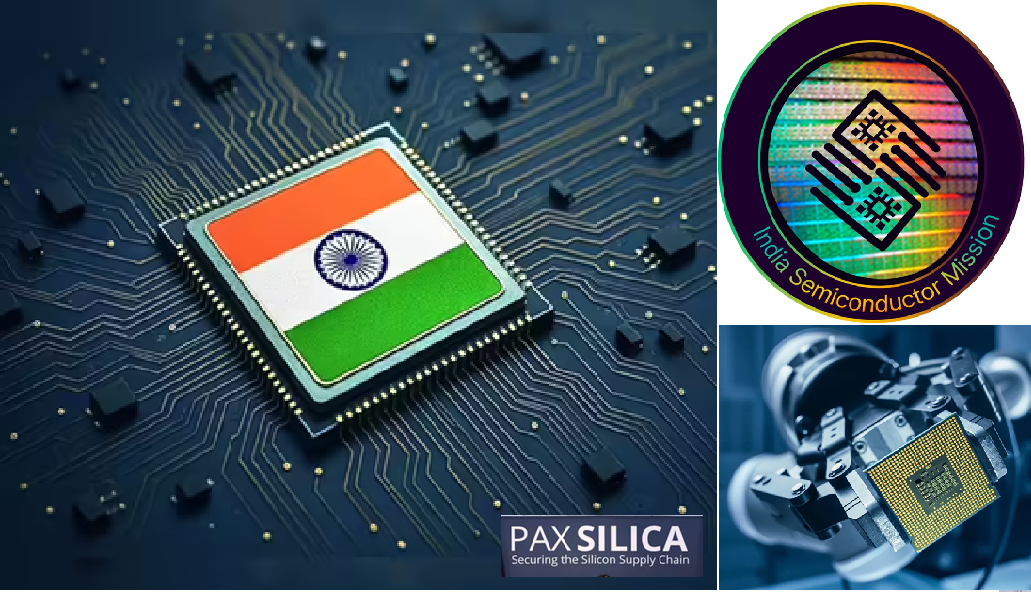
In today’s geopolitical environment, “Pax Silica” has become a significant term to describe the world order driven by controlling the world’s most essential material for technology, silicon (the new oil). As the world develops away from relying on carbon to silicon, semiconductors have emerged as valuable resources. Each nation is rushing to establish supply chains for semiconductors, with these nations separated into opposing sides in this competition. India must navigate this new world order to achieve industrial objectives, but also to maintain its strategic goals in order to protect its digital sovereignty and strengthen its economy.
The Dawn of Pax Silica and India’s Ascendance
The Pax Silica initiative is a strategy spearheaded by the US and its allies to develop a safe Trusted ecosystem for semiconductors, AI and critical minerals. At the time of the formal announcement of Pax Silica in late 2025, India had a weak position in regard to the initiative. India has a large digital market as well as being a Quad partner, but not part of the founding group of countries (Japan, South Korea, and the UK), brought to light an important weakness for India; there was a lack of a well established semiconductor fabrication (fab) operations and India’s reliance on high-quality imported silicon.
However, the narrative has shifted rapidly. By February 2026, the realisation that a global silicon order is incomplete without India’s scale and talent has led to a formal invitation for India to join the pact. India is no longer just a consumer; it is positioning itself as a “trusted geography” for the global value chain. The Indian semiconductor market, valued at approximately $39.5 billion in 2025, is on a high-growth trajectory, projected to reach $100–110 billion by 2030. This growth is underpinned by the India Semiconductor Mission (ISM), which has already approved projects worth over $19 billion (₹1.6 lakh crore) across several states, signalling India’s transition from policy formulation to active production.
iCET 2.0: The Engine of Strategic Synergy
The link between India’s domestic aspirations and the global Pax Silica is found within the U.S.-India Initiative on Critical and Emerging Technology (iCET) framework, which is now in Phase 2.0, frequently referred to as the TRUST (Transforming the Relationship Utilising Strategic Technology) initiative. This methodology has transitioned from a number of high-level conversations to a detailed roadmap for deep industrial collaboration.
iCET 2.0 is focused on eliminating the ‘regulatory cholesterol’ that has historically affected hi-tech commerce between Washington and New Delhi. Specifically, the framework allows for an enhanced level of collaboration, such as the U.S. Space Force partnership with Indian start-up 3rdiTech to establish the first-of-its-kind multi-material fabrication plant in India. The multi-materials created at this facility will be used to fabricate high-power, high-voltage electronics and sensors utilising current technologies such as Silicon Carbide (SiC) and Gallium Nitride (GaN) that have both environmental (green energy) and defence (modern warfare) applications. iCET 2.0 aligns India ISM with U.S. CHIPS and Science Act legislation, allowing India to be an equal partner/collaborator (co-developer) in the T technologies developing over the next decade rather than a secondary market.
From Design Hub to Manufacturing Powerhouse
India’s traditional strength has always been in chip design, hosting nearly 20% of the world’s semiconductor design engineers. However, under the “Pax Silica” strategy, India is aggressively moving into the “Midstream” and “Downstream” segments of the value chain.
Fabrication & ATMP: With five major production units currently under construction, including the Tata-PSMC fab in Dholera, India, it is building the physical infrastructure to move beyond the drawing board
Semicon 2.0: The recently announced ISM 2.0 (budgeted for FY 2026-27) shifts focus toward industry-led research and the creation of indigenous Intellectual Property (IP). The goal is no longer just to “Make in India” using foreign licenses, but to develop “Indian-owned” chip architectures.
Talent Pipeline: To sustain this growth, India has initiated a massive program to train 85,000 engineers in specialised semiconductor and VLSI (Very Large Scale Integration) technologies, ensuring that the “human capital” of Pax Silica remains firmly rooted in the subcontinent.
Geopolitical Insurance and Strategic Autonomy
India benefits from participating in the Pax Silica framework via iCET 2.0 in that it enjoys “strategic insurance”. As tech exports increasingly become tools of coercion, India, being a part of a trusted network, grants access to cutting-edge manufacturing capabilities and materials that are otherwise under tight export controls.
At the same time, while India has a very deep partnership with the United States, it is maintaining its Strategic Autonomy by developing its own “full-stack” ecosystem to minimise any single country’s vulnerability to Export Controls. The push for “Aatmanirbhar” semiconductors is an initiative to ensure that India’s critical infrastructure (i.e., 5G networks, defence systems, a fleet of Electric Vehicles) will be powered by secure and validated chips.
Challenges on the Horizon
While the progress is good, there are many challenges to overcome on this journey. There’s still a huge deficit of high-purity silicon domestically processed in India, as well as critical minerals such as lithium and gallium. On top of that, India is competing with many other countries; while Indian companies will work with 28nm-40nm nodes (which are the workhorses for automotive/IOT), other companies across the world have already taken the lead by manufacturing at the 2nm node. To successfully navigate Pax Silica, India’s infrastructure (in particular, its infrastructure for reliable power supply and ultra-pure water) must be capable of supporting the intensive requirements of advanced fabrication processes.
Conclusion: The Silicon Sentinel
The globalisation semiconductor race from a passive observer to a key participant, as iCET2.0 is being leveraged strategically for international cooperation with ISM2.0 being focused domestically, earning India the title of “Silicon Sentinel” in the Indo-Pacific region. Joining the Pax Silica alliance does not simply mean India has gotten to have a place to sit at the table, but rather has built its own table with a vision for future technologies that are both democratic and decentralised as well as advanced.
References
- Pax Silica – United States Department of State
- India to Join Pax Silica – MP-IDSA
- India Semiconductor Mission: Home
- Press Information Bureau (PIB) – Budget 2026-27 Announcements
- First India-US National Security Fab – The Financial Express
- India Semiconductor Mission 2.0 – PIB Detailed Note
- Joint Statement on iCET – White House Archives
Hridbina Chatterjee is a final-year postgraduate student in International Relations at Jadavpur University, Kolkata. She has written for newspapers and think tanks, with interests in South Asian politics, India’s foreign policy, and the Indo-Pacific. Views expressed are the author’s own.